Friday, October 23, 2020
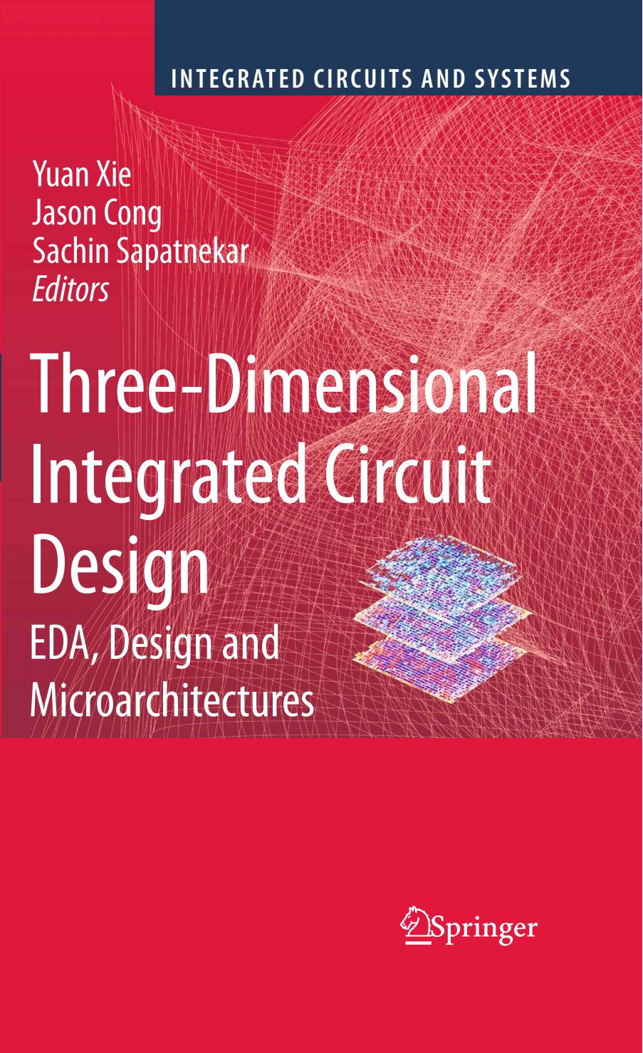
Three-Dimensional Integrated Circuit Design EDA, Design and Microarchitectures by Yuan Xie, Jason Cong and Sachin Sapatnekar
1 Introduction
2 3D Process Technology Considerations
3 Thermal and Power Delivery Challenges in 3D ICs
4 Thermal-Aware 3D Floorplan
5 Thermal-Aware 3D Placement
6 Thermal Via Insertion and Thermally Aware Routing in 3D ICs
7 Three-Dimensional Microprocessor Design
8 Three-Dimensional Network-on-Chip Architecture
9 PicoServer: Using 3D Stacking Technology to Build Energy Efficient Servers
10 System-Level 3D IC Cost Analysis and Design Exploration
To the observer, it would appear that New York city has a special place in the hearts of integrated circuit (IC) designers.
Manhattan geometries, which mimic the blocks and streets of the eponymous borough, are routinely used in physical design: under this paradigm, all shapes can be decomposed into rectangles, and each wire is either parallel and perpendicular to any other. The advent of 3D circuits extends the analogy to another prominent feature of Manhattan – namely, its skyscrapers – as ICs are being built upward, with stacks of active devices placed on top of each other. More precisely, unlike conventional 2D IC technologies that employ a single tier with one layer of active devices and several layers of interconnect above this layer, 3D ICs stack multiple tiers above each other. This enables the enhanced use of silicon real estate and the use of efficient communication structures (analogous to elevators in a skyscraper) within a stack.
Going from the prevalent 2D paradigm to 3D is certainly not a small step: in more ways than one, this change adds a new dimension to IC design. Three-dimensional design requires novel process and manufacturing technologies to reliably, scalably, and economically stack multiple tiers of circuitry, design methods from the circuit level to the architectural level to exploit the promise of 3D, and computer-aided design (CAD) techniques that facilitate circuit analysis and optimization at all stages of design. In the past few years, as process technologies for 3D have neared maturity and 3D circuits have become a reality, this field has seen a flurry of research effort.
The objective of this book is to capture the current state of the art and to provide the readers with a comprehensive introduction to the underlying manufacturing technology, design methods, and computer-aided design (CAD) techniques. This collection consists of contributions from some of the most prominent research groups in this area, providing detailed insights into the challenges and opportunities of designing 3D circuits.
The history of 3D circuits goes back many years, and some of its roots can be traced to a major government-funded program in Japan from a couple of decades ago. It is only in the past few years that the idea of 3D has gained major traction, so that it is considered a realistic option today. Today, most major players in the semiconductor industry have dedicated significant resources and effort to this area. As a result, 3D technology is at a stage where it is poised to make a major leap. The context and motivation for this technology are provided.
About المثقف
MEP Engineering Café is a free search engine which allows you to search, preview and download of PDF files into your devices.
Electrical
التسميات:
Electrical
Subscribe to:
Post Comments (Atom)


No comments:
Post a Comment